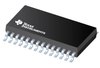
Texas Instruments recommends a specific layout and routing for the CDCV855PW to minimize noise and ensure optimal performance. A 4-layer PCB with a solid ground plane and a separate power plane is recommended. Additionally, keep the input and output traces short and away from each other to reduce noise coupling.
The output capacitor value depends on the output voltage, output current, and desired ripple voltage. A general rule of thumb is to choose a capacitor with a value between 10uF to 47uF. However, it's recommended to consult the Texas Instruments application notes and perform simulations to determine the optimal capacitor value for your specific application.
Although the datasheet specifies a maximum input voltage of 5.5V, it's recommended to limit the input voltage to 5V to ensure reliable operation and prevent damage to the device. Exceeding the maximum input voltage can lead to reduced performance, increased power consumption, or even device failure.
To ensure stability, follow the recommended layout and routing guidelines, and make sure to decouple the input and output pins with suitable capacitors. Additionally, choose a suitable output capacitor value and ensure that the output voltage is within the recommended range. If oscillations occur, try adding a small series resistor (e.g., 10Ω) between the output and the load to dampen the oscillations.
The typical startup time for the CDCV855PW is around 10ms to 20ms, depending on the input voltage, output voltage, and load conditions. However, this time can vary depending on the specific application and design. It's recommended to consult the datasheet and application notes for more information.