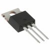
The BD911 can operate from -40°C to 150°C, making it suitable for high-reliability applications.
To ensure proper biasing, connect the VCC pin to a stable voltage source between 4.5V and 18V, and the GND pin to a solid ground plane. Also, decouple the VCC pin with a 10uF capacitor to reduce noise.
To minimize electromagnetic interference (EMI) and ensure reliable operation, keep the BD911 away from high-current paths and noisy signals. Use a solid ground plane, and route the input and output signals as close to the device as possible.
Use a voltage regulator or a transient voltage suppressor (TVS) to limit the input voltage to the recommended range. Also, add a current-limiting resistor or a fuse in series with the input to prevent overcurrent conditions.
Use a standard SO-8 footprint with a land pattern that provides a solid connection to the device pins. Ensure the PCB layout allows for easy thermal dissipation and minimizes thermal resistance.